Characterization of the interface between highly conductive Ga:ZnO films and the silicon substrate
Resumen
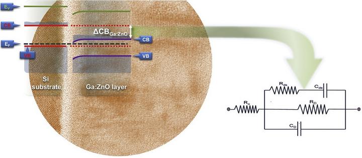
Gallium-doped zinc oxide films are an interesting alternative for transparent conductive materials. To improve their performance, the interface between the grown layer and the substrate must be fully understood. Accordingly, ZnO and Ga:ZnO films have been deposited onto p-type doped Si (111) substrates by magnetron sputtering for 1, 2, 3 and 20 min and their interfaces characterized by transmission electron microscopy, photoelectron spectroscopy, spectroscopic ellipsometry and impedance spectroscopy. The combination of transmission electron microscopy techniques suggested a more complex interface chemistry in the Ga:ZnO/Si case, a point confirmed by x-ray photoelectron spectroscopy measurements on very thin films. While the ZnO/Si interface consists mostly of silicon oxides, zinc silicates and some Zn0, the Ga:ZnO/Si interface, besides these constituents, has a noticeable amount of Ga:ZnO and small quantities of Ga0. The band alignment deduced from the photoelectron spectroscopy measurements, together with the layers and Si band gap values, evidences a higher work function for the doped film and a smaller conduction band barrier for the Ga:ZnO/Si interface. Concerning the optical and electrical characteristics, spectroscopic ellipsometry revealed no significant differences between the two interfaces, while impedance spectroscopy measurements demonstrated that the Ga:ZnO/Si interface is less resistive than the ZnO/Si one.
Full citation
M. Gabás, E. Ochoa-Martínez, E. Navarrete-Astorga, A. R. Landa-Cánovas, P. Herrero, F. Agulló-Rueda, S. Palanco, J. J. Martínez-Serrano, and J. R. Ramos-Barrado,
“Characterization of the interface between highly conductive Ga:ZnO films and the silicon substrate,”
Appl. Surf. Sci. 419, 595–602 (2017).
DOI: 10.1016/j.apsusc.2017.05.072