🔬 Lab#
Intro#
In 1995 I started the Raman Microscopy Laboratory for the study and characterization of materials by Raman microspectroscopy.
See my notes on Raman microspectroscopy.
I am specially interested in nanomaterials and microestructured materials, i.e., with inhomogeneities of the order of a few micrometers in composition, orientation, stress, crystallinity, etc.
Experimental equipment#
The lab started with the acquisition of a Renishaw Ramascope 2000 Raman microspectrometer, with the possibility of point by point spectral mapping (confocal microscopy with lateral and depth resolution).
Excitation wavelength: 514.5 nm (green) and 633 nm (red)
Spectral resolution: 3 cm-1
Spatial resolution: 0.6 μm (in the green)
Publications#
See the page of papers for a compilation of published results.
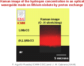
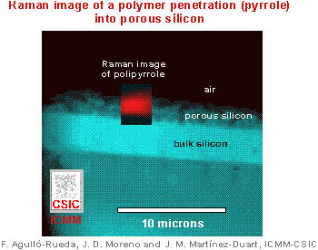
Examples#
The following figures illustrate the application of Raman microscopy to chemical imaging in materials science. The data were obtained at the Raman Microscopy Lab of the Materials Science Institute of Madrid, CSIC, in collaboration with other groups.
Contents: