🏠 Home#






🚶️ Biography#
Fernando Agulló-Rueda is a Senior Research Scientist in the Nanocarma research group at the Materials Science Institute of Madrid (ICMM), part of the Spanish National Research Council (CSIC), where he has worked since 1988. He earned his Ph.D. in Physics from the Autonomous University of Madrid (UAM) in 1986, with a focus on halide perovskites. Following his doctorate, he spent four years conducting research abroad: eight months at the University of Hamburg establishing a Raman spectroscopy laboratory, over two years at the IBM Thomas J. Watson Research Center in New York, and one year at the Max-Planck Institute for Solid State Research in Stuttgart, Germany. At IBM and Max Planck, he investigated the electro-optical properties of semiconductor nanostructures.
Agulló-Rueda has dedicated his career to studying the optical properties of materials, authoring more than 138 peer-reviewed publications with over 4,000 citations [h-index = 33 (WOS), h-index = 39 (Google Scholar)]. He has also authored several books, including Electrooptics, Nanotechnology for Microelectronics and Optoelectronics, and Fundamentos de microelectrónica, nanoelectrónica y fotóníca.
In 1995 he established the Raman Microscopy Lab at ICMM to investigate the nano- and microstructure of materials and devices. He has collaborated extensively with other research groups in diverse fields such as optical waveguides, semiconductor nanostructures, thin films and coatings, biological materials, and the effects of ion and laser irradiation.
Beyond his research, Agulló-Rueda is committed to science communication and education, contributing to outreach through courses, books, and book chapters. He has supervised three doctoral theses at UAM and is an active member of various scientific societies. He has served for over two years on the Executive Council of the Spanish Vacuum Society (ASEVA) , where he held the role of Treasurer.
Download
resumé
😍️ Interests#
Materials science
Optical properties
Raman microscopy
Micro- and nanostructure
Optical spectroscopy
Materials characterization
Optical and vibrational properties
Nanomaterials
Thin films and coatings
Semiconductors
Metallic oxides
Radiation effects
👨🎓️ Education#
🎓️ PhD in Physics, 1986, Autonomous University of Madrid (UAM)
🎓️ MSc in Physics, 1982, Autonomous University of Madrid (UAM)
🎥️ Experience#
- Senior Research ScientistJun 2006 – Present Madrid, Spain


Raman microscopy of micro- and nanomaterials. In charge of the Raman Microscopy Lab. Setup of a homemade Raman microspectrometer. Principal investigator of various research projects. Studied the relationship between microstructure and properties of photonic materials like semiconductors and optical waveguides produced by ion irradiation. Studied biological materials (natural and artificial silk fibers). Lecturer in the on-line Master on advanced materials and nanotechnology (UAM) and the on-line Interuniversity Master on Plasma, Laser and Surface Technologies (UCO-UPM).
- Visitor scientistJan 1991 – Dec 1991 Stuttgart, Germany


With Prof. Holger T. Grahn, in the groups of Prof. Klaus von Klitzing and Prof. Klaus Ploog. Studying the optical and electro-optical properties of complex GaAs/AlGaAs semiconductor superlattices.
- Research AssociateFeb 1988 – Jun 2006 Madrid, Spain


Studied porous silicon, semiconductor nanostructures and photonic materials like LiNbO3 waveguides and CdTe thin films by Raman spectroscopy. Established a new Raman Microscopy Lab in 1995. Lecturer at the Autonomous University of Madrid (UAM) (Undergraduate course Analytical mechanics for Chemistry, 1 semester). Lecturer of the Course on Science and engineering of the surface of metallic materials (Spanish Center for Metallurgical Research, CENIM).
- Postdoctoral scientistSep 1987 – Dec 1989 Yorktown Heights, New York, USA


With Prof. Emilio E. Mendez, in the group of Prof. Leo Esaki and Prof. Leroy L. Chang. Effect of electric fields on the optical properties of semiconductor nanostructures like GaAs/AlGaAs and CdTe/CdMnTe semiconductor superlattices. Running and upgrading a lab on semiconductor spectroscopy with Spex double monochromators, liquid helium cryostat and Ar ion, Kr ion and Ti-sapphire lasers. Observation of the Wannier-Stark ladder and electric-field induced doubly-resonant Raman effect.
-


With Prof. Jörg P. Kotthaus. Setup of a new Raman microspectroscopy laboratory for the study of semiconductor nanostructures at different temperatures (10–300 K) and variable excitation wavelengths in the near infrared with a dye laser and an argon ion laser. The Raman spectrometer was one of the first Dilor XY models, with a diode array detector and many options: macro/microscope collection, triple monochromator with the first two working either in subtractive or additive mode. The Dilor XY was one of the first commercial systems for Raman microscopy.
-


PhD student under the supervision of Prof. José Manuel Calleja. Internal vibrations of molecular groups as a probe of local crystal structure and phase transitions. Raman spectroscopy of halide perovskites and halide hydrates as a function of temperature and high hydrostatic pressure. Use of Jarrell Ash 25-300 double monochromator with photomultiplier tube, liquid nitrogen cryostat and diamond anvil cell.
PhD. Thesis title: “Espectroscopía Raman de cristales con grupos moleculares NH4MX3 y MX2·H2O (Raman spectroscopy of crystals with molecular groups NH4MX3 and MX2·H2O)”. [educacion.gob.es]. [Dialnet].
🍾️ Accomplishments#
-
The objective of ASEVA is to stimulate research and scientific collaboration in the fields of vacuum science, techniques and applications including related multi-disciplinary topics as solid-vacuum interfaces.
- 19th International Conference on Thin Films (ICTF2023)Sep 2023 – Sep 2023
The 19th International Conference on Thin Films (ICTF2023), organized by the Spanish Vacuum Society (ASEVA) , was held in Burgos (Spain), September 26–29th, 2023
- 2022 Iberian Vacuum Meeting / Reunión Ibérica de Vacío (RIVA XII)May 2022 – May 2022
The Iberian Vacuum Conference (Reunión Ibérica de Vacío, RIVA XII) was a joint meeting of the Portuguese Vacuum Society (SOPORVAC) and the Spanish Vacuum Society (ASEVA) held in Braga, Portugal, May 16–117th, 2022
- Oct 2021 – Oct 2021
The Iberian Vacuum Conference (Reunión Ibérica de Vacío, RIVA) is a joint meeting of the Portuguese Vacuum Society (SOPORVAC) and the Spanish Vacuum Society (ASEVA)
 h-index : 33 (Web of Science)Jan 1982 – Mar 2025
Total number of citations to my articles (Citations) = 4 028
 h-index = 39 (Google Scholar)Jan 1982 – Oct 2025
Total number of scientific articles citing my articles (Citations) = 6 111
- Jan 1983 – Jan 2012
A total of six 6-year periods of research activity approved by peer review
-
spectroscopyNOW was an internet portal with news, tutorials, and links on spectroscopy, established by the publisher John Wiley and Sons. I was the editor of the Raman spectroscopy channel from its foundation in 2001 until 2005.
-
Grant for a postdoctoral stay at IBM Thomas J. Watson Research Center in Yorktown Heights, New York, USA. The Spanish Microelectronics Program was an initiative to foster the science and industry of microelectronics in Spain.
-
Grant to realize a doctoral thesis at the Autonomous University of Madrid (UAM)
📚 Books#
For a full list of coauthored and contributed books click here
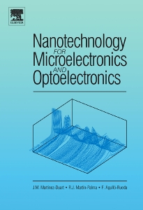
J. M. Martínez-Duart, R. J. Martín-Palma, and F. Agulló-Rueda, Nanotechnology for Microelectronics and Optoelectronics (Elsevier, 2005).
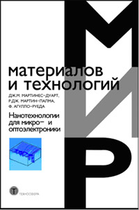
Мартинес-Дуарт Дж. М., Мартин-Палма Р.Дж., Агулло-Руеда Ф., Нанотехнологии для микро- и оптоэлектроники (РИЦ Техносфера, москва, 2007). In Russian.
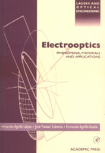
F. Agulló-López, J. M. Cabrera, and F. Agulló-Rueda, Electrooptics: Phenomena, Materials and Applications (Academic Press, New York, 1994).
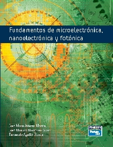
J. M. Albella Martín, J. M. Martínez-Duart, and F. Agulló-Rueda, Fundamentos de microelectrónica, nanoelectrónica y fotónica (Fundamentals of microelectronics, nanoelectronics and photonics) (Pearson Educación, Madrid, 2005). In Spanish.
📰️ Scientific articles#
For a full list of publications click here
📰️ Featured articles#
E. E. Mendez, F. Agulló-Rueda, and J. M. Hong, “Stark Localization in GaAs-GaAlAs Superlattices under an Electric Field,” Phys. Rev. Lett. 60, 2426–2429 (1988).
H. Ohno, E. E. Mendez, J. A. Brum, J. M. Hong, F. Agulló-Rueda, L. L. Chang, and L. Esaki, “Observation of Tamm States in Superlattices,” Phys. Rev. Lett. 64, 2555–2558 (1990).
F. Agulló-Rueda, E. E. Mendez, and J. M. Hong, “Quantum coherence in semiconductor superlattices,” Phys. Rev. B (Rapid Communications) 40, 1357–1360 (1989).
F. Agulló-Rueda, E. E. Mendez, and J. M. Hong, “Doubly Resonant Raman Scattering Induced by an Electric Field,” Phys. Rev. B 38, 12 720–12 723 (1988).
V. Barranco, M. A. Lillo-Rodenas, A. Linares-Solano, A. Oya, F. Pico, J. Ibañez, F. Agulló-Rueda, J. M. Amarilla, and J. M. Rojo, “Amorphous Carbon Nanofibers and Their Activated Carbon Nanofibers as Supercapacitor Electrodes,” J. Phys. Chem. C 114 10302-10307 (2010).
B. Ballesteros, G. de la Torre, C. Ehli, G. M. Aminur Rahman, F. Agulló-Rueda, D. M. Guldi, and T. Torres, “Single-wall carbon nanotubes bearing covalently linked phthalocyanines - Photoinduced electron transfer,” J. Am. Chem. Soc. 129, 5061–5068 (2007).
O. de Melo, F. Agulló-Rueda, and V. Torres-Costa, “Spatially resolved MoOx phases by laser localized oxidation of MoO2: A possible route for all-molybdenum-oxide devices,” J. Mater. Chem. C 9, 6579–6588 (2021).
F. Agulló-Rueda, N. Gordillo, M. D. Ynsa, A. Maira, J. Cañas, and M. A. Ramos, “Lattice damage in 9-MeV-carbon irradiated diamond and its recovery after annealing,” Carbon 123, 334–343 (2017).
M. Elices, G. Guinea, G. Plaza, C. Karatzas, C. Riekel, F. Agulló-Rueda, R. Daza, and J. Pérez-Rigueiro, “Bioinspired fibers follow the track of natural spider silk,” Macromolecules 44 (5), 1166–1176 (2011).
F. Agulló-Rueda, E. E. Mendez, B. Bojarczuk, and S. Guha, “Raman Spectroscopy of Wurtzite InN Films Grown on Si,” Solid State Comm. 115, 19–21 (2000).
📰️ Most recent articles#
Y. Mendez-González, J.D.S. Guerra, F. Agulló-Rueda, O. Peña‐Rodríguez, A. Fernández García, M. Manso Silvan, “Evolution of the structural and optical properties of La doped silver niobate-based thin films,” Mater. Sci. Eng. B 323(A), 118667 (2026).
P. Camarero, E. Rincón, P. Haro-González, F. Agulló-Rueda, A. García-Cabañes, M. Carrascosa, “Light-induced Accumulation of Micro- and Nano-Plastics from Water Dispersion by Optoelectronic Lithium Niobate Platforms,” Adv. Mater. Interfaces 12, e00462 (2025).
I. Solana, M. Dolores Ynsa, F. Agulló-Rueda, J. Sánchez-Prieto, D. Grojo, J. Siegel, and M. Garcia-Lechuga, “Silicon amorphization responses by combined irradiations with MeV ion beams and ultrashort laser pulses,” Surf. Interfaces 69, 106772 (2025).
J. de Damborenea, A. Conde, G. P. Rodriguez-Donoso, F. Agulló-Rueda, and M. A. Arenas, “Thermal shock resistance of additive manufactured Inconel 718 by concentrated solar energy,” Scientific Reports, 15, 7557 (2025).
R. Magro, A. Muñoz-Noval, J. A. Briz Monago, J. R. Murias, A. Espinosa Rodríguez, L. M. Fraile, F. Agulló-Rueda, M. D. Ynsa, C. Tavares de Sousa, B. Cortés Llanos, G. M. García López, E. Nacher, V. García Tavora, N. Mont i Geli, A. Nerio, V. Valladolid Onecha, R. Pallás, A. Tarifeno-Saldivia, O. Tengblad, M. J. Manso Silvan, and S. Viñals i Onsés, “Iodine substituted hydroxyapatite nanoparticles and activation of derived ceramics for range verification in proton therapy,” J. Mater. Chem. B 12, 12030–12037 (2024).
N. Naveas, R. Pulido, T. Graber, R. Martin-Palma, F. Agulló-Rueda, I. Brito, M. Á. García, M. T. Sevilla, J. Hernandez-Montelongo, A. Muñoz-Noval, C. Marini, L. Soriano, J. Sánchez-Marcos, and M. Manso Silvan, “Experimental and theoretical investigation of the treatment of Cu-rich acid mine drainage using iron oxide magnetic nanoparticles,” J. Environ. Chem. Eng. 12, 113822 (2024).
A. Fernández García, R. Ariza, J. Solis, F. Agulló-Rueda, M. Manso Silvan, and M. Garcia-Lechuga, “Out-of-plane growth of 2D molybdenum diselenide nanosheets on ultrafast laser-structured substrates,” Appl. Surf. Sci. 669, 160567 (2024).
Y. Mendez-González, F. Agulló-Rueda, V. Torres-Costa, A. Fernández García, J. D. S. Guerra, and M. Manso Silvan, “Influence of the synthesis method on the microstructural properties of Ta modified AgNbO3 ferroelectric thin films,” Curr. Appl. Phys. 59, 10 (2024).
A. Fernández García, M. Garcia-Lechuga, F. Agulló-Rueda, J. Rubio Zuazo, and M. Manso Silvan, “Femtosecond laser thinning for resistivity control of tungsten ditelluride thin-films synthesized from sol-gel deposited tungsten oxide,” Surf. Interfaces 44, 103668 (2024).
For a full list of publications click here
