F. Agulló-Rueda
F. Agulló-Rueda
🏠 Home
📰 Publications
📚 Books
🔬 Lab
📒 Tutorials
👨🏫 Teaching
💬 Outreach
🥳 Fun
📩 Contact
Light
Dark
Automatic
🇺🇸 English
🇪🇸 Español
temperature
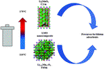
Hydrothermal control of the lithium-rich Li$_2$MnO$_3$ phase in lithium manganese oxide nanocomposites and their application as precursors for lithium adsorbents
Dalton Trans.
50
(31), 10765–10778 (2021)
R. Pulido
,
N. Naveas
,
T. Graber
,
R. Martín-Palma
,
F. Agulló-Rueda
,
I. Brito
,
C. Morales
,
L. Soriano
,
L. Pascual
,
C. Marini
,
J. Hernandez-Montelongo
,
M. Manso Silvan
Cite
DOI
Lattice damage in 9-MeV-carbon irradiated diamond and its recovery after annealing
Carbon
123
, 334–343 (2017)
F. Agulló-Rueda
,
N. Gordillo
,
M. D. Ynsa
,
A. Maira
,
J. Cañas
,
M. A. Ramos
Cite
DOI
Micro-Raman spectroscopy of near-surface damage in diamond irradiated with 9-MeV boron ions
We have studied the near-surface damage in a diamond crystal caused by irradiation with swift boron ions and its healing after …
F. Agulló-Rueda
,
M. D. Ynsa
,
N. Gordillo
,
A. Maira
,
D. Moreno-Cerrada
,
M. A. Ramos
Cite
DOI
Laser heating induced phase changes of VO$_2$ crystals in air monitored by Raman spectroscopy
We have studied the effect of intense visible light on vanadium dioxide crystals in air by measuring micro-Raman spectra for increasing …
P. Vilanova-Martínez
,
J. Hernández-Velasco
,
A. R. Landa-Cánovas
,
F. Agulló-Rueda
Cite
DOI
Optical and structural properties of Sb$_2$S$_3$/MgF$_2$ multilayers for laser applications
Multilayers of MgF
2
and Sb
2
S
3
have been obtained by physical vapour deposition on glass substrates. Changes in the optical and …
F. Perales
,
F. Agulló-Rueda
,
J. Lamela
,
C. de las Heras
Cite
DOI
Optical and structural properties in the amorphous to polycrystalline transition in Sb$_2$S$_3$ thin films
Sb$_2$S$_3$ thin films have been obtained by physical vapour deposition on LiNbO$_3$ and glass substrates. Films with amorphous …
F. Perales
,
G. Lifante
,
F. Agulló-Rueda
,
C. de las Heras
Cite
DOI
Compositional Study of LiNbO$_3$ Thin Films Grown by Liquid Phase Epitaxy
Lithium niobate (LN) films have been obtained on pure congruent single-domain LN substrates by the liquid phase epitaxy technique. …
D. Callejo
,
S. Manotas
,
M. D. Serrano
,
V. Bermúdez
,
F. Agulló-Rueda
,
E. Diéguez
Cite
DOI
Laser Heating in Porous Silicon Studied by Micro-Raman Spectroscopy
We have measured the temperature rise in nanoporous silicon under strong illumination. A green laser beam was focused with a microscope …
S. Manotas
,
F. Agulló-Rueda
,
J. D. Moreno
,
F. Ben-Hander
,
R. Guerrero-Lemus
,
J. M. Martínez-Duart
Cite
DOI
Depth-Resolved Microspectroscopy of Porous Silicon Multilayers
Appl. Phys. Lett.
75
, 977–979 (1999)
S. Manotas
,
F. Agulló-Rueda
,
J. D. Moreno
,
R. J. Martín-Palma
,
R. Guerrero-Lemus
,
J. M. Martínez-Duart
Cite
DOI
Effect of Thermal Annealing on Te Precipitates in CdTe Wafers Studied by Raman Scattering and Cathodoluminescence
A combination of Raman scattering and cathodoluminescence techniques has been used to study the spatial distribution of Te precipitates …
N. V. Sochinskii
,
M. D. Serrano
,
E. Diéguez
,
F. Agulló-Rueda
,
U. Pal
,
J. Piqueras
,
P. Fernández
Cite
DOI
»
Cite
×